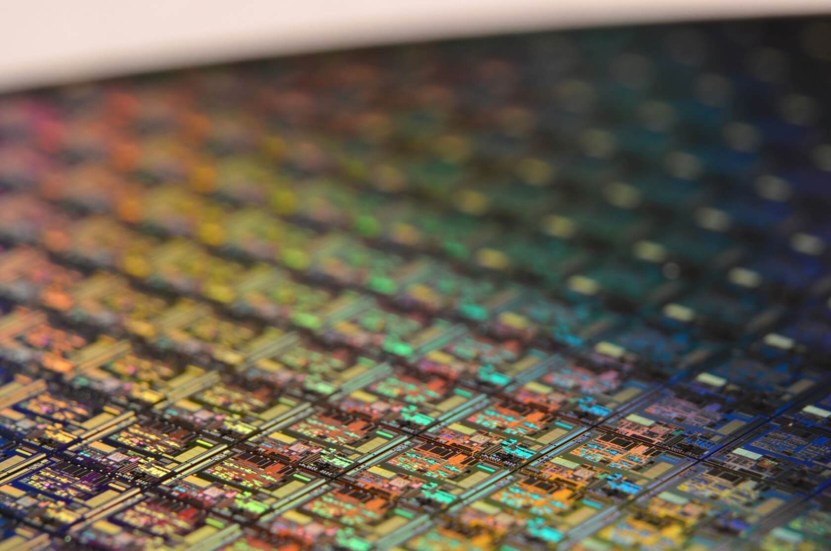
Highly anticipated: TSMC's long awaited N7+ (7nm+) process that uses extreme ultraviolet lithography on critical layers is now ramping into commercial availability, and customers should be shipping products based on N7+ soon. What's more, TSMC's clients should be taping out designs for 6nm early next year. This will be a continuation of TSMC's EUV process that will increase transistor density, expand the use of EUV across more layers, and lower manufacturing costs and complexity.
TSMC announced that it's bringing its N7+ EUV process node to the market in high volume, and it bears the distinction of being the first commercially available 7nm, EUV-based process technology.
TSMC's N7+ is derived from the original N7 process, as TSMC has kept the tools, IP and infrastructure between the nodes highly portable. This will also help with the shrink to 6nm and 5nm, both of which are currently set for risk production. The N6 process slated for volume production by the end of 2020. The N7+ process entered volume production last May, but is ramping up to commercial availability just in time for high profile clients like AMD to put orders in for 2020.
TSMC notes that the N7+ process is among the fastest the company has ever recorded thanks to excellent yield learning, already matching yields of the original N7, which debuted in the form of Apple's A12 Bionic SoC. TSMC also goes on to say that its EUV tools have reached full production maturity, hitting target goals for volume production and uptime, as well as managing output power of greater than 250 watts for daily operations. All of this bodes well for the future migration to the N6 and N5 processes, each of which will use EUV in more layers.
When weighed against the N7 process that uses deep ultraviolet lithography, N7+ is set to deliver a 15% to 20% increase in density and improved power efficiency. TSMC is currently pivoting to deploy capacity to meet demand; reports already suggest that TSMC has extended its lead time for 7nm due to insatiable demand. N7+ is likely to see similar popularity, as we've known for some time that AMD plans to use TSMC's 7nm+ process for its Zen 3-based Ryzen chips.
Apple will also continue to be a prominent partner for TSMC. With its most recent A13 Bionic SoC, it isn't clear if Apple elected to use TSMC's N7+, or the iterative N7P node that Apple was rumored to be considering. We know that Huawei is using the N7+ process for its latest Kirin 990 5G SoC.
In other foundry news, TSMC is currently locked in a litigation battle with foundry peer GlobalFoundries, with both companies alleging patent infringement.
