
Forward-looking: During Samsung's Foundry Forum 2022, the company revealed a roadmap for processor sizes within various Samsung devices. Samsung Foundry's presentation went in-depth regarding the next five years of the roadmap, giving enthusiasts a glimpse into the near future of mobile computing.
Samsung has long been one of the leading developers of semiconductors and processors, including being the first foundry to produce 3nm chips for its mobile devices. The company beat out its biggest rival, TSMC, to the 3nm node, certainly not a small feat even for such a large fabricator.
Every year, Samsung holds a Foundry Forum event, usually detailing plans and roadmaps for numerous Samsung devices and collaborations with other industries. One of the company's main focuses this year is the roadmap for its processors and subsequent node sizes. With rival TSMC revealing its hopes to have mass production of 2nm chips by the end of 2025, Samsung decided to present its roadmap up to 2027.
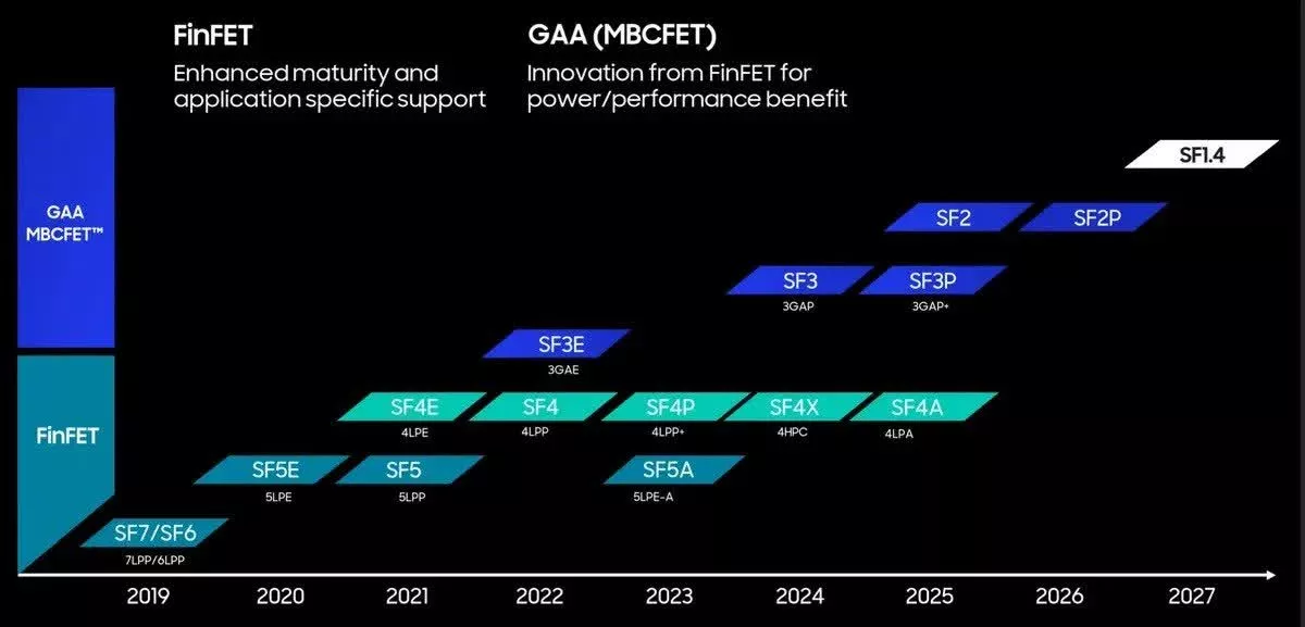
The roadmap states that Samsung plans to have an updated "2nd-gen" 3nm process node available in 2024. Samsung Foundry CEO Siyoung Choi claims that the updated 3nm process will feature 20 percent smaller transistors, allowing for better power efficiency in devices that use Samsung's processors.
Samsung plans to improve the design of its 2nm node slated for mass production in 2025. Its goal is to increase performance by moving power delivery to the backside of the processor. Intel expects to introduce a similar feature dubbed PowerVia to some of its processors by 2024.
The final update to the roadmap was the announcement of the upcoming 1.4nm node, expected to be available in 2027. It did not cover specific improvements for these chips. After all, we are talking about plans that are five years out and subject to change. However, seeing the size slowly inch closer to the even smaller picometer range is exciting.

Samsung expects over 50 percent of the demand for its processors to come from the automotive, HPC, IoT, and 5G markets. It currently produces 28nm eNVM chips for automotive clients but hopes to reduce this node size to 14nm eNVM soon and 8nm eNVM later.
All in all, it's a fascinating time to be a tech enthusiast as companies continue to push the boundaries of processing chips. Who will be the first to reach chip sizes in the picometer range? Only time will tell, but we're certainly excited to see.