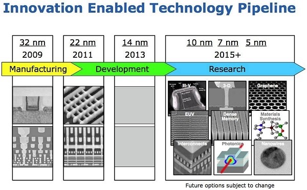
Intel spoke a great deal about their next generation Haswell processor earlier this week at IDF but the latest bit of information to emerge from the show has to do with the 22nm manufacturing process as well as next year's 14nm die shrink.
Director of process technology Mark Bohr said their 22nm manufacturing process has exceeded expectations. The company's new tri-gate transistor technology that debuted in Ivy Bridge processors earlier this year also received praise. Bohr explained that the transistors' leakage and sub-threshold slope were more efficient than Intel had anticipated. As such, the technology will likely be extended to a couple more generations.

Work on the 14nm process shrink is also coming along swimmingly but it's not without its own set of hurdles. In 22nm tri-gate technology, the transistor pitch (the distance between two transistors) is 80nm. This also happens to be the smallest pitch possible using single-pattern lithography so in order to go even smaller, Intel has to use double patterning to obtain tighter pitches.
Additional steps in the lithography process will add extra cost but according to Bohr, that expense won't be passed on to the consumer. Improved density will offset the additional wafer cost and allow Intel to continue to reduce the per transistor cost.
The 14nm manufacturing process is currently on track for production around the end of next year but of course we probably won't see chips built on the process until sometime in 2014.