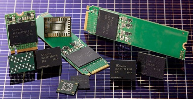
Something to look forward to: SK Hynix has joined the 96-layer club, launching the "world's first 96-layer 512Gb (gigabit) CTF-based 4D (four dimensional) NAND flash" memory. The 4D NAND flash moves from company's previous 72-layer tech to 96-layers, allowing the chips to be 30 percent smaller and with a 49 percent increase in productivity per wafer.
Toshiba and Samsung are just two of the companies that have started manufacturing 96-layer NAND products. SK Hynix's chip is based on its TLC (Triple-Level Cell) arrays, using 3D CTF (Charge Trap Flash) design, rather than floating gate, and its logic circuitry is placed underneath the flash cells---a design it calls Periphery Under Cell (PUC). Other companies use a similar technique but under different names. Samsung calls it Core Over Periphery, and Micron's version is CMOS Under the Array.

SK Hynix said the 4D NAND chips bring a 30 percent higher write and 25 percent higher read performance compared to its 72-layer 512Gb 3D NAND. Data bandwidth, meanwhile, is doubled to 64KB, the industry's biggest. "With the introduction of a multiple gate insulators architecture, its data I/O (Input Output) speed reaches 1,200Mbps (Megabits/sec) at 1.2V (Volt) of operation power," the company wrote.
SK Hynix plans to introduce 1TB SSDs that use its 4D flash tech along with its own controllers and firmware within the year, with enterprise SSDs arriving in the second half of 2019. The company added that it would also release "ultra-high density" 96-Layer 1Tb triple-level cell (TLC) and quad-level cell (QLC) SSDs in 2019.
"This 96-Layer CTF-based 4D NAND, with the industry's top cost competitiveness and performance, will become a milestone in the company's NAND flash business, as a platform in developing future products," said JT Kim, company VP and head of NAND marketing. "The company plans to start the early stage mass production of it within this year and further expand the production in M15 to actively respond to a variety of clients."
