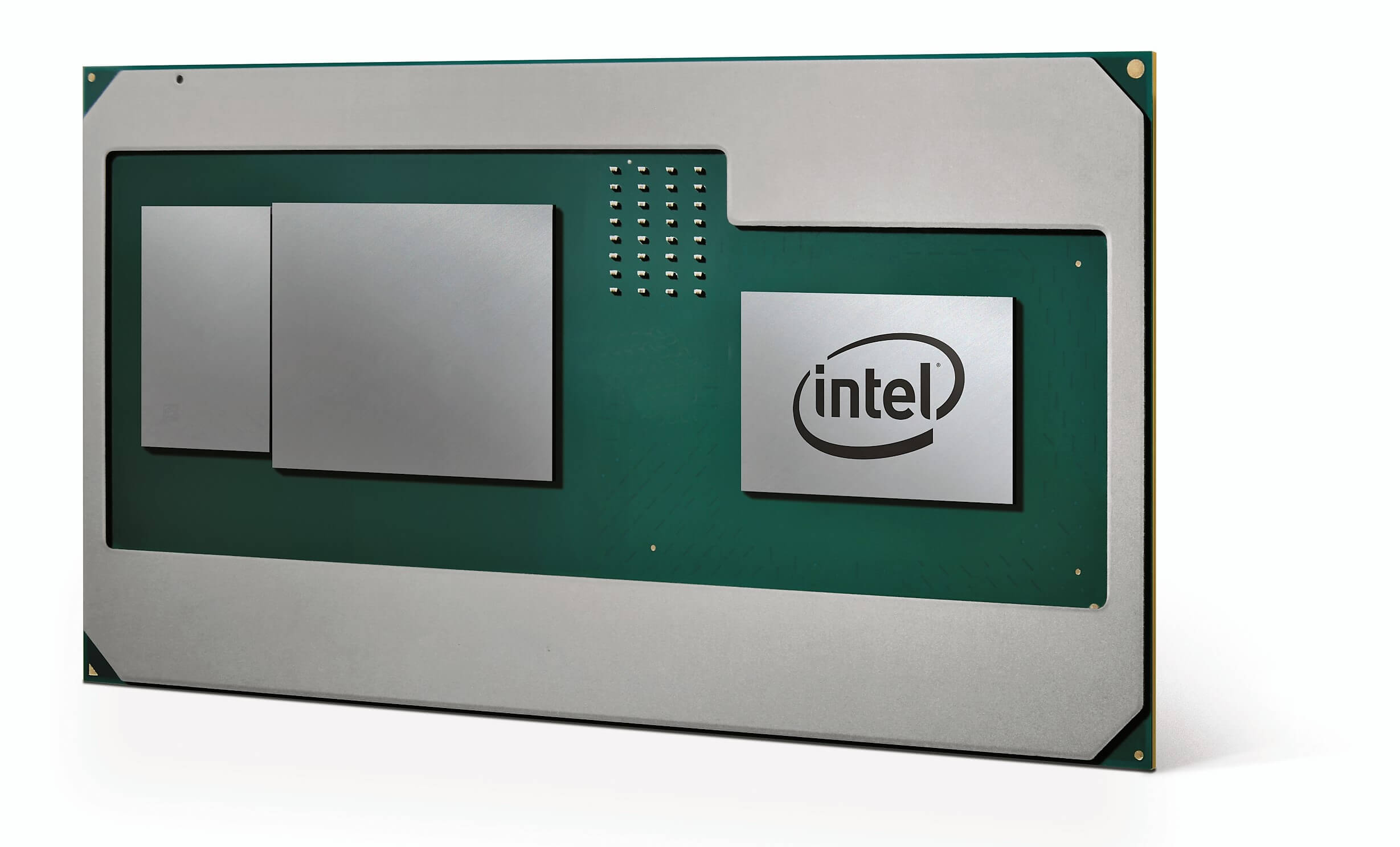
Forward-looking: What do Intel foundries and Legos have in common? Not much, right now. But if Intel delivers on a future of mix 'n' match pieces of silicon, then we'll see multiple silicon IP blocks patched together with Intel's proprietary technology.
Riding on the coat tails of the successful Kaby Lake-G development, Intel has been pressing home the message that future chip designs will be heterogeneous instead of monolithic, in what it's calling "mix and match innovation."
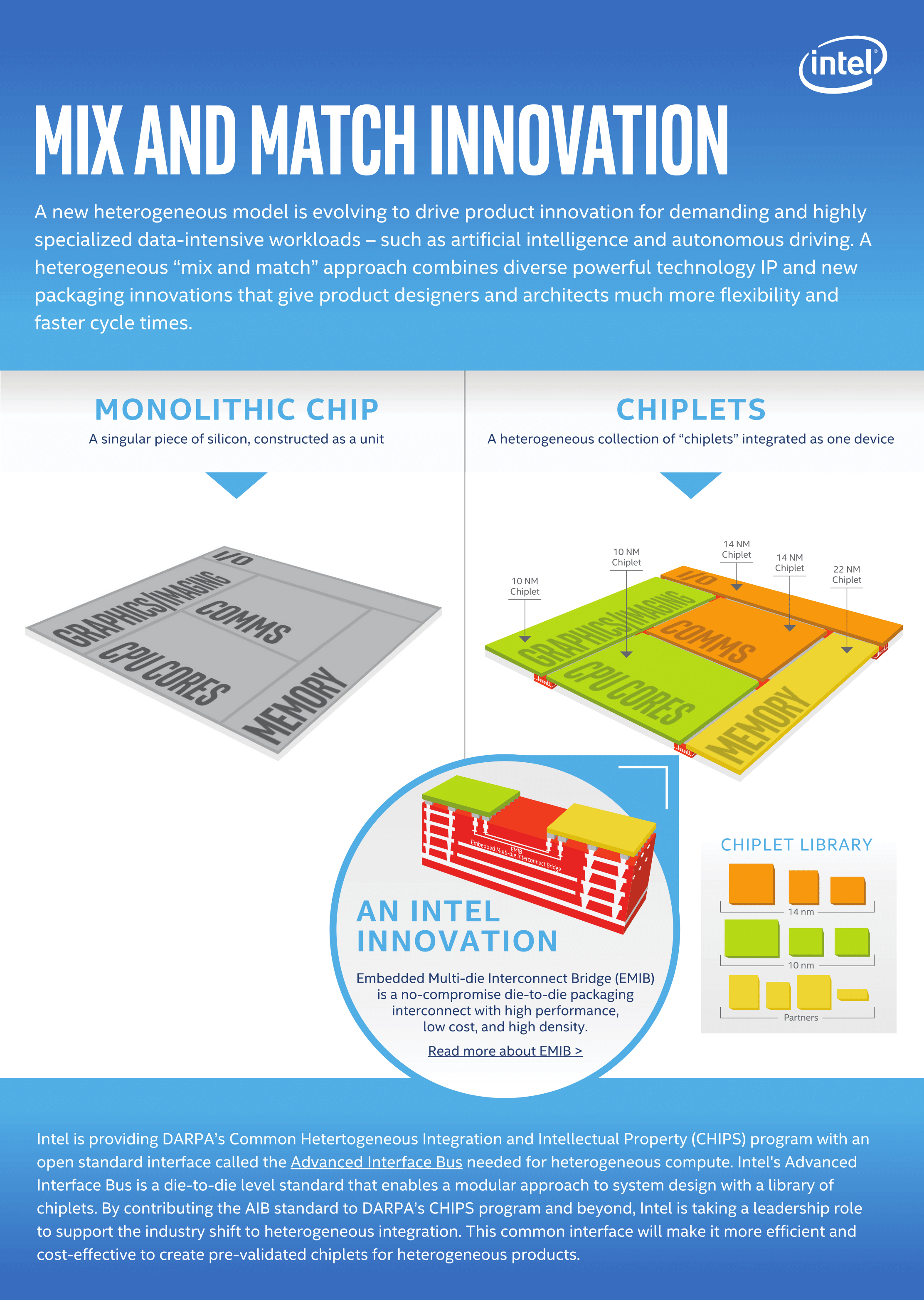
The company's plan translates into adopting multiple pieces of silicon known as chiplets, interconnected using EMIB interconnects, combining multiple pieces of silicon from a pre-approved "chiplet library," to create a highly-custom silicon design.
The chiplet library is, in essence, a repository of pre-designed chip elements (or IP blocks), such as I/O, memory subsystem, communications, CPU and GPU silicon, which have been designed to use a common interface which interconnects them on a single package, yet with performance close to that of a monolithic design, as defined by DARPA in its Common Heterogeneous Integration and IP Reuse Strategies (CHIPS).

The idea is that you can stick together different pieces of silicon (hence the "Mix 'n' Match"), which needn't even be manufactured at the same fab or share the same process node, and have them communicate under a single common interface.
Intel, on its side, is taking the opportunity at Hot Chips to oblige and talk up its recent successes, hoping to capitalize on industry momentum.
Claiming the technical and political high-ground with Kaby Lake G and its Stratix 10 designs, Intel is jumping on the opportunity, having even created a dedicated specification for an Advanced Interface Bus (AIB) and given it away to DARPA, in the hopes it will become the standard interface for CHIPS-compliant designs and aid its foundry business unit (Intel Custom Foundry), which so far has had difficulty in finding customers outside its parent company.

According to Intel, its process hands-down beats the competition's "2.5D" approach, as it builds the connections without the need for Through-Silicon Vias (TSVs), simplifies design and does not change the package yield, which in Fab economics, is worth a great deal. The competition, such as TSMC's CoWoS and InFO, have alternatives to Intel's process, but they are initially more expensive and add process steps to the assembly of the chips.
Interestingly, AMD has recently shown its own alternative to on-die communication, and suggested this is all much ado about nothing.
So what does it all mean? There is an industry-wide movement towards highly-custom, integrated and heterogeneous chip designs which will most likely lead to a faster cadence of chips, higher versatility and lower manufacturing costs, all good things if the savings and features are passed onto the consumer.
