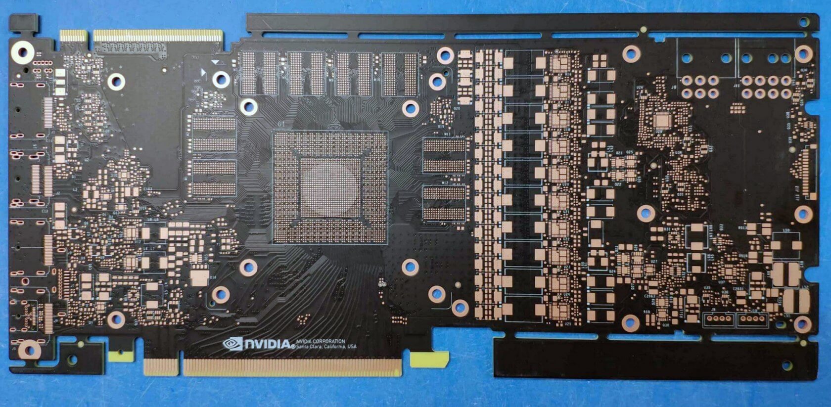
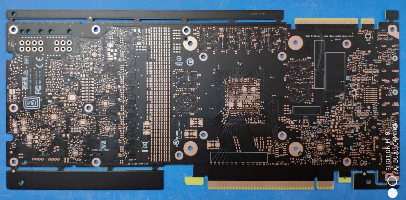
Highly anticipated: With the promise of "some spectacular surprises" in store, it looks as if we'll finally get to see Nvidia's long-awaited GTX 1180 (or whatever it's called) at Gamescom on August 20. Now, two alleged photos said to show the graphic card's PCB could give us an idea of what to expect ahead of the event.
The photos come courtesy of a Baidu user, so, as is always the case with these sort of things, a dose of salt is advised. Images of the printed circuit board reveal some interesting details. The eight memory dies placed around the GPU core suggest it will feature either 8GB or 16GB of VRAM, which is presumed to be of the GDDR6 variety.
We also see a 10-phase VRM powered by 6+8 pin power connectors---more than the GTX 1080's single 8-pin connector. This setup matches the GTX 1080 Ti's 6-pin and 8-pin PCI Express power connectors.

The different SLI fingers could suggest Nvidia is implementing an NVLink connector in place of SLI in the GTX 1180, something it does in its enterprise cards such as the Quadro GV100. This offers higher bandwidth than SLI or PCIe for card-to-card communications.

The GPU pin size suggests the presence of the GV104 processor, and one of four video-out connectors is smaller than the others, which could hint at the presence of USB Type-C. MSI was first to add a Type-C port to a GPU, in its GTX 1080 Ti Gaming X Card from last year.
Finally, the PCB shows a 256-bit bus interface and Nvidia's logo on the bottom, meaning this is likely a final reference PCB rather than a custom model. We'll likely find out the accuracy of the photos at Gamescom in just over two weeks' time.
