The Taiwan Semiconductor Manufacturing Company, better known as TSMC, is holding its 24th annual Technology Symposium in Santa Clara right now, and it's just unveiled a process that could spell a revolution for graphics cards: Wafer-on-Wafer (WoW) technology.
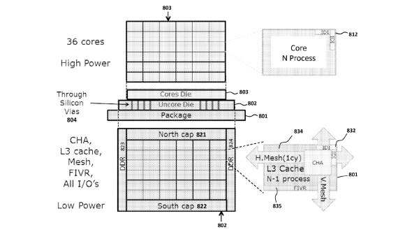
As the name suggests, WoW works by stacking layers vertically rather than placing them horizontally across a board, much like how 3D NAND flash memory is stacked in modern solid-state drives. What this means is more powerful GPUs for Nvidia and AMD without the need to increase their physical size or shrink the fabrication process.

The back-to-back wafers make contact with each other through the use of 10-micron holes that form a through-silicon via (TSV) connection. TSMC partner Cadence explains that WoW designs can be placed onto an interposer---an electrical interface that routes one connection to another---creating a 2-die cube. It's even possible to vertically stack more than two wafers using the WoW method.
The technology will allow more cores to be crammed into a single package and means each wafer can communicate with each other extremely quickly and with minimal latencies. What's especially interesting is the way WoW could be used by manufacturers to place two GPUs on a single card and release it as a product refresh, creating what is essentially two GPUs in one without it appearing as a multiple GPU setup to the operating system.
The biggest issue with WoW right now is the wafer yields. As they are bonded together, if just a single wafer is bad then both have to be discarded, even if there's no problem with the other one. This means the process would need to be used on production nodes with high yield rates, such as TSMC's 16nm process, in order to be cost efficient. However, the company aims to use WoW with future 7nm and 5nm fabrication processes.

